Electron microscopes use beams of electrons rather than beams of light to produce highly magnified images of specimens. These versatile devices come in different types and are used for a variety of applications.
The first microscopes used light to magnify objects. Called optical microscopes, they are still widely used today, but their resolving power is limited by the wavelength of light. The best optical microscopes can magnify no more than about 2000 times. Electrons have a much smaller wavelength (the de Broglie wavelength, from quantum theory’s prediction that all particles have wave-like characteristics). Electron microscopes can magnify objects up to 2 million times, a resolution three orders of magnitude finer than that of light microscopes.
While optical microscopes use lenses made of transparent, light-refracting material to bend light, the electron beams used in electron microscopes do not pass through any physical material. Since electrons are charged particles, they respond to electromagnetic forces, so electron microscopes use magnetic fields to bend the electron beams.
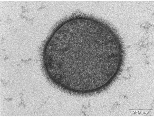
Below left: Transmission electron micrograph of a bacillus bacterium.
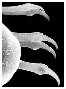
Below right: Scanning electron micrograph of the chaetae (bristles) of a ploychaete worm
Transmission Electron Microscopes
Transmission Electron Microscopes
The first electron microscope was a transmission electron microscope (TEM), which dates to 1938. In a TEM, the beam of electrons, focused by electrostatic and electromagnetic lenses, enters the specimen. The electrons interact with the specimen, with some electrons passing through it and others being scattered. The result is a two-dimensional image of the interior of a specimen.
For viewing by a transmission electron microscope, samples are prepared by sectioning usng a diamond knife on an ultramicrotome, with the resulting slices less than 100 nm thick. Just as samples are chemically stained for viewing under an optical microscope, specimens for TEM may be stained with heavy metals that scatter the electron beam.
Scanning Electron Microscopes
In a scanning electron microscope (SEM), the electron beam is directed to move across the surface of the specimen so as to map the entire specimen field. This “map” is called a raster pattern. The electrons interact with the surface and experience several different effects. Detectors send the resulting information to a computer, which processes it and produces an image. Scanning electrom microscopes have great depth of field and yield striking three-dimensional images. A SEM image includes information only about the surface of an object, since the electron beam does not penetrate the specimen.
The effects experienced by electrons in a SEM provide different kinds of information about the sample. The main means in of gathering information in SEM is s_econdary electrons_, which are electrons generated by primary radiation, in this case the electron beam. Also, different materials emit X-rays in specific spectra when exposed to electromagnetic radiation, so detecting and analyzing these characteristic X-rays provides information about the atomic composition of the sample.
Other Electron Microscope Techniques
In some scanning electron microscopes, the principle of cathodoluminescence is used. This effect occurs when a beam of electrons strikes a semi-conducting surface and is used most commonly in conventional television sets, but it can also be used in SEM when special optical detectors are incorporated into the device. This principle is most useful in materials science and mineralogy applications. Since the surface must be a semi-conductor, cathodoluminescence can be used to study only non-metallic substances.
Back-scattering of electrons is analogous to reflected and refracted light; electrons retain the same energy but change direction when they encounter the surface. Because they have wavelike properties, the electrons can interfere with each other – that is, they can increase or decrease each others’ wavelengths. These effects are used in reflection high energy electron diffraction (RHEED), in which electrons are directed at a crystal surface at a shallow angle to gather information about that surface.