The stubborn, cumbersome, low efficiency traditional types of thick-film solar panels are today slowly being replaced by more promising thin film solar panels. What technology and components make them so impressive? Let’s find out!
Thick-Film vs Thin Film Solar Panels
Thin-film semiconductor technology- an invention which was specifically intended for computers- is now finding a significantly important application in PV (photovoltaic) cells, especially in the production of thin film solar roof panels. Precisely speaking, the term “thin film” doesn’t necessarily refer to the reduced thickness of the component; rather it’s because of the inclusion of many thin consecutive layers of atoms and molecules to build up the layer.
Thin-film technology has the following advantages over traditional thick-film solar panel technology:
- Thin-film has a reduced cross-sectional area compared to conventional counterparts.
- This facilitates making them flexible and less cumbersome, thus allowing them to be produced continuously in a large area process.
- The finished product is very light in weight and can be easily maneuvered and installed on building roofs.
- Because of their super light weight, they are more favorable and compatible with solar trackers .
- Continuous development in its technology is helping them to become more efficient than the thick-filmed solar panels.
Manufacturing Thin Film Solar Panels
Two criteria must be primarily satisfied for manufacturing thin film solar cells. One is to find a proper substrate, and the second to select a poly-Si thin film layering or depositing technique.
In order to meet the above requirements, SSP (Silicon Sheets from Powder) equipment and RTCVD (Rapid Thermal Chemical Vapor Deposition) system installations are done.
Countries like China are the leading producers of metallurgical Si powder. This is exported and sold at very low costs, and thus becomes significantly beneficial for the easy preparation of SSP for manufacturing poly-Si thin film solar panels.
10% efficiency may not look very impressive, however for developing countries, it can be very helpful considering the huge costs involved with the manufacturing of the higher efficiency counterparts.
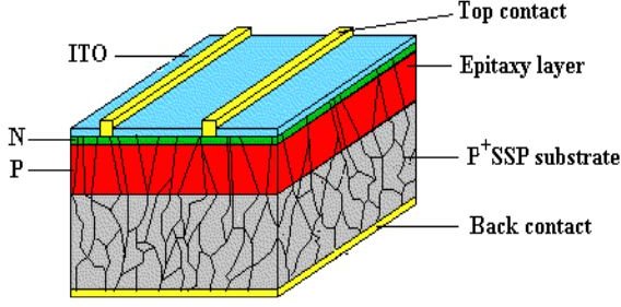
Let’s try to understand the basic ingredients that make up the basic structure of a poly-Si thin film solar cell over SSP through the following discussion. Looking at the figure alongside, we see that it’s typically made up of 5 discrete layers viz:
- The uppermost contact made up of Indium Tin Oxide (ITD)
- The thin N-type doped section (green color), and the rather prominent P-type doped section (red color) also called the epitaxy layer
- The intermediate base material P+SSP substrate and the extreme back contact shown in yellow color.
The above explained structure of SSP layer has three fundamental functions:
- To self support the operation of the device
- Carrying out crystal seed growth for the epitaxial layer and
- Maintain BSF or back surface field for enhancing the properties of the solar cell (open circuit voltage VOC)
In the process of manufacturing firstly over the SSP base the epitaxial layer is made through RTCVD (hopefully in the future the intermediate layers will also include material like SiO2 to improve solar cell efficiency), after that the pn junction is introduced by a diffusion process.
The ITO contact elements are fixed through a process of vacuum evaporation and finally an antireflection cover of SiNX film is coated over the surface through PECVD.
After concluding the above process, the SSP ribbon is subjected to the following procedures:
- Silicon powder is heavily injected and packed continuously over the quartz carrier plates by electric motor
- The upper surface powder of the layer is introduced to a temperature of about 14120 Celsius and is zone melted in a special Ar atmosphere through high intensity line focused halogen lamps
- The remaining silicon powder gets combined with the molten liquid during the process of re-crystallization
The above manufactured solar cell ribbon is very thin typically 0.6 to 1mm in thickness (depending upon the silicon powder particle size) and 60 to 110mm wide and normally the length is about 1000 to 1500mm.
The finished product is sleek, flexible, rollable, and perfectly suited as thin film solar roof panels.
Wondering where to buy these thin film solar panels? Perhaps the list of manufacturers provided here should help.
Conclusion
The application of thin film silicon is the most important factor for developing a high class response from these solar cells.
RTCVD becomes suitable especially because firstly SSP substrate is selected and secondly a bigger grain size becomes obtainable.
Trichlorosilane (SiHCL3) is preferred which is a cheaper version of Si resource.
The chemical thermal reaction is expressed through the following equation:
SiHCL3 + H2 = Si
The involvement of RTCVD particularly facilitates bigger application area, obtaining larger grain size, and enforcing low cost potentials.